Electronic PCB Design
A PCB breathes life into your product concept. We undertake simple to complex designs on rigid, flexible and flex-rigid PCBs.
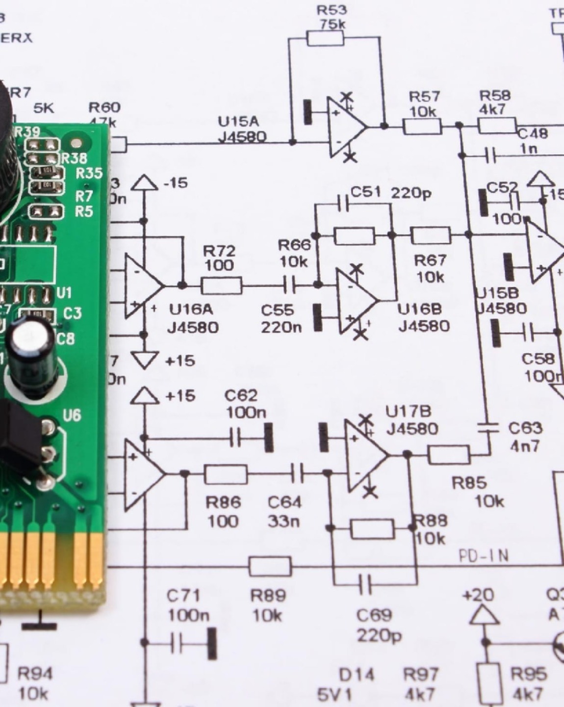
Our design service begins with the creation of a conceptual circuit design which is converted into a schematic design using various 3D CAD tools at our factory in Suffolk UK. The schematic represents the components and the connections between them. This design element is fundamental for verifying basics such as pin numbering, labels, symbols, connectors, decoupling capacitors and so on.
The next phase of our PCB circuit board design is circuit board layout where the Bill of Materials (EBOM) is developed from the schematic, and long lead time and obsolete components are identified. As a skilled PCB design company, we can undertake product re-engineering to manage parts obsolescence.
Where there is sufficient space on the board, We try to use larger size components for ease of assembly but space, current, voltage, frequency and availability play their part in the selection of components.
Additionally at this stage, the stack-up design is an important attribute which defines the structure of multilayer circuit boards. The schematic design, EBOM and stack-up design are the backbone of the electronic circuit design developed by our UK team.
PCB Design Services
Your Custom PCB Circuit Board Optimised for Manufacture
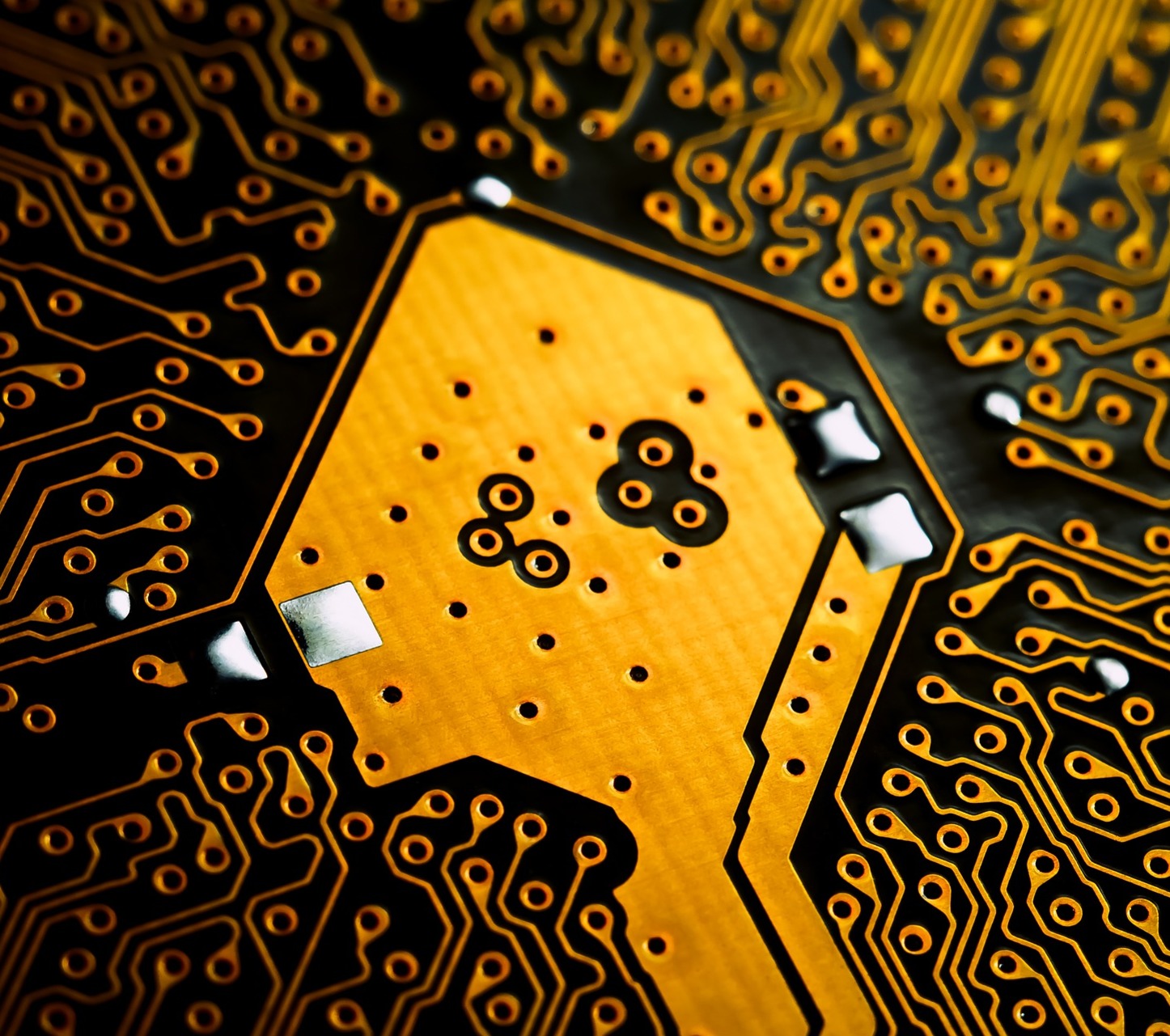
Our deep understanding of thermal management, electro-magnetic interference, and component placement, ensures the PCB layout is fully optimised for manufacturing.
Design for testing is an important consideration; we incorporate test points for all important signals to ensure signal integrity on critical signal paths.
We often produce PCB prototypes to test not only the PCB but also the complete product prototype for proving the fundamental concept at the lowest possible cost.
Whilst we will usually assemble, test and deliver the production PCB’s, we can supply the production assembly drawings and all files required for costing, procurement and manufacture.

CUSTOM UK PCB

ELECTRONICS PROTOTYPING

PCB MANUFACTURING


